|
|
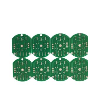
Technology & Capabilities
|
|
1. Product Range
|
Rigid PCBs from 2- 24 layers, HDI; Aluminium base
|
|
2. Min. Board Thickness
|
2 layer
|
4 layer
|
6 layer
|
8 layer
|
10 layer
|
|
min. 0.2 mm
|
0.4 mm
|
1 mm
|
1.2 mm
|
1.5 mm
|
|
12 & 14 layer
|
16 layer
|
18 layer
|
20 layer
|
22 & 24 layer
|
|
1.6 mm
|
1.7 mm
|
1.8 mm
|
2.2 mm
|
2.6 mm
|
|
3. Max. Board Size
|
610 x 1200 mm
|
|
4. Base Material
|
FR-4 Glass Epoxy laminate, Aluminium base, RCC
|
|
5. Surface Finish Treatment
|
Electroless nickel Immersion gold ( Electoless Ni/Au). Organic Solerability Preservatives ( OSP or Entek). Hot Air Leveling ( Lead- Free, RoHS). Carbon Ink. Peelable Mask. Gold Fingers. Immersion Silve. Immersion Tin. Flash gold ( Electrolytic)
|
|
6. Major Laminate
|
King Boad (KB-6150). ShengYi (S1141; S1170). Arion. YGA-1-1; Rogers and others.
|
|
7. Via Holes
|
Copper PTH/ Blind Via/ Buried Via/ HDI 2+N+2 with IVH
|
|
8. Copper Foil Thickness
|
18um/ 35um/ 70um~245um (outer layer 0.5oz~7oz)
18um/ 35um/ 70um~ 210um (inner layer 0.5oz~6oz)
|
|
9. Min. Via Size and Type
|
Dia. 0.15mm (Finished).
Aspect Ratiao = 12; HDI holes (<0.10mm)
|
10. Min. Line Width & Spacing
|
0.75 mm/ 0.10mm ( 3mil/ 4mil)
|
|
11. Min Via Hole Size & Pad
|
Via: Dia, 0.2mm/ pad. dia. 0.4mm; HDI<0.10mm via
|
|
12. Impedance I Control Tol.
|
+/- 10% ( min. +/- 7 Ohm)
|
|
13. Solder Mask
|
Liquid Photo- Image (LPI)
|
|
14. Profiling
|
CNC Routing, V- Cutting, Punching, Push back punching, Connector chamfering
|
|
15. Capacity
|
100 k㎡ output monthly
|
FAQ:
Question 1.Are you pcba factory?
Answer:yes of course.
Question 2:Does your factory provide one stop service?
Answer:Yes of course we have purchase department and designer.
Question 4:can you provide me sample to test before mass order?
Answer:Yes of course
Question 5:how about your package?are you sure that i will receive the prefect goods without damage?
Answer:we provide custom foam box to protect the product.